About
 My background encompasses twenty years of leadership, innovation and technology development in semiconductor and adjacent markets such as Augmented Reality, 3D Sensing, Advanced Optics, Display, Battery and Solar. This includes:
Latest Research Areas
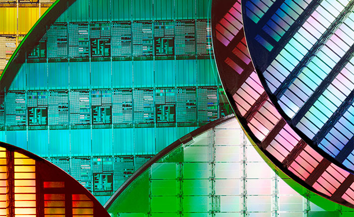
Semiconductor

Optics / Augmented Reality

Materials Engineering
Blog News
New Patent Granted – March 6th 2018
US 9,911,594: Selective atomic layer deposition process utilizing patterned SAM for 3D structure application

Social Media